

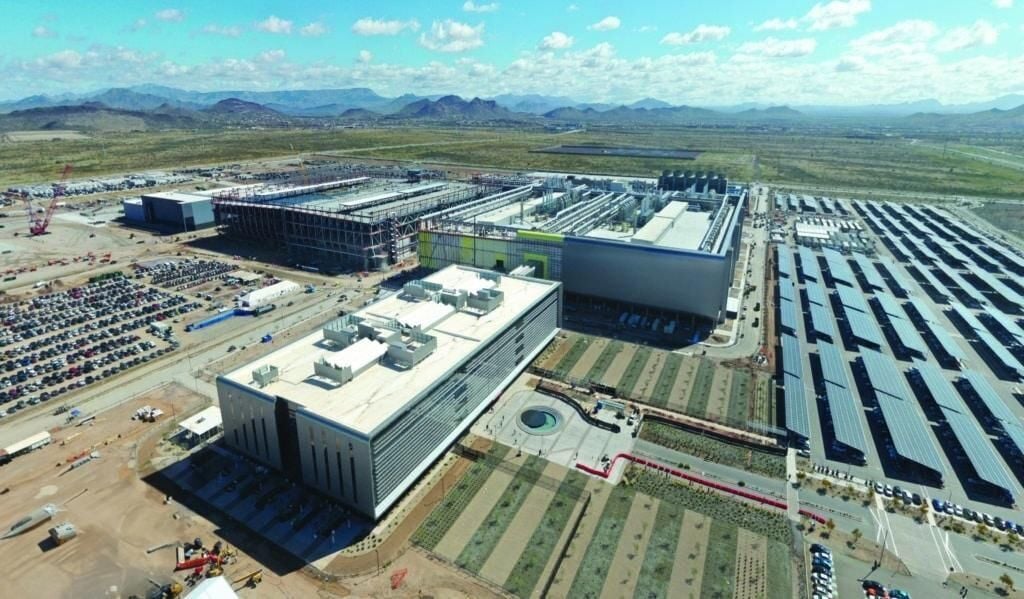
Taiwan Semiconductor Manufacturing Company has reached a groundbreaking moment in American industrial history with its third fabrication facility ceremony in Arizona, marking another significant milestone in the company’s $165 billion investment in semiconductor manufacturing in the United States. Construction for the TSMC Arizona project officially commenced in late April 2025, establishing what is recognized as the most significant foreign direct investment in the nation’s history.
Accelerated Development Strategy
The TSMC Arizona initiative has demonstrated exceptional momentum by advancing its construction timeline for the third fab. Initially planned for construction in 2026, the company moved the groundbreaking forward to 2025, reflecting its commitment to expanding U.S. production capacity amid potentially growing demand for advanced semiconductors. This expedited schedule follows TSMC’s board meeting held on American soil for the first time in the company’s 37-year history in February 2025, highlighting the potentially increasing strategic importance of its U.S. operations.
State-of-the-Art Technology Integration
The newest facility will manufacture chips using 2-nanometer or more advanced process technology, with production potentially scheduled to begin by the end of this decade. This TSMC Arizona installation joins the company’s first Arizona fab, which started volume production of 4-nanometer chips in late 2024, and a second fab currently under construction that will focus on advanced 2-nanometer technology with next-generation nanosheet transistors, targeted for production in 2028.
These facilities distinguish themselves through exceptional scale, featuring cleanroom areas approximately double the size of a typical logic fab. This expanded capacity is designed to accommodate the extensive equipment required for leading-edge production, potentially positioning the complex at the forefront of semiconductor manufacturing technology in the United States.
Comprehensive Packaging Solutions
The company is expanding its U.S. presence through advanced packaging capabilities that extend beyond chip fabrication. In October 2024, TSMC signed an agreement with Amkor Technology to collaborate on advanced packaging at Amkor’s planned $2 billion facility in Peoria, Arizona. The partnership focuses on TSMC’s Integrated Fan-Out (InFO) and Chip on Wafer on Substrate (CoWoS) packaging technologies, which are critical for smartphone applications and artificial intelligence GPUs.
The proximity of TSMC Arizona’s front-end fabs and Amkor’s back-end facility is designed to accelerate overall product cycle times, potentially creating a more integrated and efficient semiconductor manufacturing ecosystem in Arizona. This collaboration addresses a crucial aspect of the semiconductor supply chain, which has been previously concentrated in Asia, allowing U.S. customers to have their chips both fabricated and packaged domestically.
Regional Economic Development
The expanded operation represents a potentially transformative investment for the region’s economy. When fully operational, the three fabs are expected to create approximately 6,000 direct high-tech jobs. The construction phase alone is anticipated to generate numerous direct construction jobs, with many additional indirect supplier and consumer jobs expected throughout this decade.
Currently employing more than 3,000 people at its Arizona campus, spanning 1,100 acres, TSMC Arizona has catalyzed the development of the broader semiconductor ecosystem. The Greater Phoenix Economic Council reports that the region has attracted 39 semiconductor-related companies, resulting in the creation of more than 7,700 jobs and over $37 billion in capital investment. This clustering effect is transforming Phoenix into what some industry observers have dubbed the “Silicon Desert.”
Investment Evolution and Federal Partnership
The investment has undergone significant changes since its initial announcement. What began as a $12 billion commitment in 2020 expanded to $40 billion in 2022, then to $65 billion in 2024 with the addition of the third fab. In March 2025, TSMC announced an additional $100 billion investment, bringing the total to $165 billion.
Significant federal incentives under the CHIPS and Science Act have supported this expansion. In November 2024, the U.S. Department of Commerce finalized an award of up to $6.6 billion in direct funding for the project, along with up to $5 billion in loans. The company is also eligible for Investment Tax Credits of up to 25% on qualified capital expenditures.
Industry Leadership and Sustainability
Major technology companies have expressed support for the project. NVIDIA’s Jensen Huang emphasized the importance of producing AI infrastructure manufacturing in America. At the same time, AMD’s Lisa Su highlighted their role as one of the first and largest high-performance computing customers for the facility. Apple has positioned itself as the largest customer at the TSMC Arizona facility, committing to sourcing chips as part of its broader $500 billion U.S. investment plan.
The campus incorporates significant sustainability measures, including a target of 90% water recycling through an advanced Industrial Water Reclamation Plant designed to achieve “Near Zero Liquid Discharge.” By the end of this decade, when all three Arizona fabs are operational, TSMC will potentially build a comprehensive semiconductor manufacturing ecosystem in the United States, thereby strengthening supply chain resilience for critical technologies and reducing dependency on offshore production.
